All about PCB reverse engineering

Shenzhen OROD is a well-known name in the field of PCB reverse engineering industries. It provides a wide range of services related to reverse engineerings such as circuit board processing, printed circuit board design, PCBA manufacturing, and many more.  Shenzhen OROD is one of the earliest PCB reverse engineering services providers in China with over 10 years of reverse engineering experience.  It has newly established an advanced PCB reverse engineering research laboratory.  Approximately 100000 circuit board reverse engineering cases are handled every year with a guaranteed success rate of the board copying cases.  Highly efficient and high success rate make this company highly praised in the circuit board industry.  

There is a defined process through which PCB reverse engineering works such as scanning a picture of the circuit board, removing the components, making BOM, grinding the plate, adjusting the contrast and shade, starting the PCB reverse engineering software Protel, converting the BMP of the top layer into TOP, Convert the BMP of the BOT layer into BOT, Compose it into a graph, Print double-sided PCB board.

PCB reverse engineering is a complicated process to perform. Though it is basically dealing with very tiny components, the tools used for this process are very sophisticated.  Below are a few of the various PCB reverse engineering tools used in this process given

Test tools

Impedance test, power supply current supply, electronic component model, test circuit board circuit. a DC power supply, a magnifying glass, a circuit detector, and an impedance tester, among others.

Polishing PCB board tools:

Mainly PCB board polishing primarily comprising sandpaper, grinding equipment, impellers, and corrosive agents.

Scanning tool:

Scan THE PCB and save the circuit diagram as a collection of images for later board duplication. Scanner, computer, printer, and caliper are the main tools.


Engineers frequently have trouble locating the drawings while repairing electronics products, especially older models. There might no longer be any circuit diagrams available at present. Drawing a circuit diagram based on the actual products is therefore required in order to analyze and improve the product. There are different processes used to execute this process few of which are given below.

1. Reasonably divide functional areas

When reverse designing the schematic diagram of an intact PCB board. Dividing up functional areas can help engineers avoid unnecessary problems. It also improves the efficiency of drawing.

In general, the same functional components on an electronic circuit board will be placed centrally. Dividing areas by function can provide a convenient and accurate basis for reverse analysis of schematics. However, the division of this functional area is not arbitrary. It requires engineers to have a certain understanding of electronic circuit related knowledge.

First, find out the core components of a functional unit, and then find out the same function according to the wiring connection,  Other elements of the unit. Form a functional partition (the formation of functional partition is the basis of schematic drawing). In addition, In this process, don’t forget to use the component number on the circuit board wisely, they can help you to partition the function faster.

2. Find the right reference components

This reference component can also be said to be the main component for reference at the beginning of schematic drawing. In determining the benchmark , The components are then drawn according to the pins of these reference components. The accuracy of schematic diagram can be guaranteed to a greater extent. For engineers, the determination of reference components is not very complicated, in general, can choose to be the main circuit.  The components to be used as reference components, they are generally larger, more pins, easy to draw, such as integrated circuits, transistors and so on. Can be used as appropriate reference components.

3. Correctly distinguish lines and reasonably draw wiring

To distinguish ground cables, power cables, and signal cables, engineers also need to have knowledge of power supplies, circuit connections, PCB wiring knowledge and so on. The distinction of these circuits can be analyzed from the connection of components, the width of copper foil and the characteristics of electronic products themselves. In cabling drawing, in order to avoid line crossing and interspersing, ground symbols can be widely used for ground cables. Various lines can use different colors of different lines to ensure clear discernable, various components can also use special signs, and even the unit circuit can be drawn separately, and then combined.

4. Master the basic framework and refer to similar schematic diagrams

For some basic electronic circuit frame composition and principle drawing method, engineers need to master, not only to be able to some Simple, classic basic composition of the unit circuit to draw directly, but also to form the overall framework of the electronic circuit. On the other hand, do not neglect that the same type of electronic products have certain similarities in the schematic diagram.  Engineers can according to the accumulation of experience, full reference to similar circuit diagram to carry out the reverse analysis of the new product schematic diagram.

5. Check and optimize

After schematic drawing is completed, testing and verification should be carried out. To calculate the PCB schematic of the reverse design end.  The marking values of components sensitive to PCB distribution parameters need to be checked and optimized, And the schematic diagram should be carried out according to the PCB file diagram Contrastive analysis and check to ensure that the schematic diagram, And document diagram are completely consistent.

PCB design documents are converted to PDF files during PCB reverse engineering analysis for simple viewing or to query related component data. There are steps to steps processes for using Altium Designer to produce a standard PDF file for getting a printed circuit board reverse engineering.

During PCB reverse engineering analysis, PCB design documents are converted to PDF files for easy viewing or for querying related component information. The following describes how to output a regular PDF file by  Altium Designer.
The preliminary work is to install the virtual printer and PDF reader on the computer. After you are ready, follow the following steps:

(1) Run the File-Intelligent PDF command to open the PDF output configuration wizard, as shown in Figure 11-25. Press Next to go to the Next step.

PCB reverse engineering to pdf

(2) Select the export target: Set the output path of the file as prompted.
(3) Export BOM of raw materials: BOM output option, this option is optional, but Altium Designer has a special BOM output function, this is generally not checked.

PCB reverse engineering to pdf

PCB reverse engineering to pdf

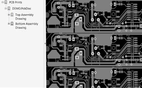
Double click “Top Layer Assembly Drawing” output column, you can set the output properties, Assembly elements generally output mechanical Layer, screen printing Layer and welding resistance Layer, click “Add” “Delete” and other buttons to add, delete and other operations related to the output Layer. Similarly, do the same for the output bar of “Bottom Layer Assembly Drawing”.

PCB reverse engineering to pdf

PCB reverse engineering to pdf-

If it is an assembly drawing, generally add the following line layer for output.

1, Top/Bottom Overlay:

2, Solder: Top/Bottom Solder.

3, Mechanical/ keep-out Layer.

PCB reverse engineering to pdf

PCB reverse engineering to pdf

PCB reverse engineering cost is affected by many complex factors.  For instance, the size of the PCB board, the number of front and back components, the number of PCB layers, the kinds of features—such as BGA, blind holes, the various PCB reverse engineering tools used, etc. The cost is various. The cost of PCB cannot be measured using a single benchmark. Skipping schematics can help you save money and time if you don’t need complicated secondary product development.

Other problems of PCB reverse engineering

In the electronic industry, PCB reverse engineering is the most common electronic product engineering technology. It is also called PCB copy and PCB clone. We can get a 1:1 PCB file, BOM list, schematic file. Some customers also need to export Gerber files for production. After the factory receives the technical documents, they can make printed circuit board and welding components. The technicians passed the test and debugging of the circuit board. Finally, we make samples and mass production.

For the PCB board we connected, the final accuracy rate of all project PCB circuit diagrams is 100%. If it is not correct, it can be modified for free until it is perfect!

The completion time cannot be precisely determined due to the number of parts, the number of welding points, the presence of blind holes, and other factors:

  • Small-size single-layer PCBs typically only require 1-2 days;
  • Typically, a two-layer small-size PCB takes two to three days;
  • Typically, it takes 3–4 days to complete a PCB with 4-6 layers;
  • It takes longer than 7 working days if the PCB has more than 8 layers and blind holes;

PCB boards or electronic products provided by customers must be legal. Our company is not responsible for the legal problems arising therefrom! At the same time, we keep the customer’s project data confidential and completely delete the project data after the handover is completed!

Welcome new and old friends to consult!

It is essential to conduct technical analysis, technical follow-up, technological barrier breakthrough, and competitive analysis of the existing popular products given the rapid upgrading of electronic products and the emergence of new foreign technology products in the information age. Reverse engineering electronics services for printed circuit boards were created as a result of this.

Shenzhen OROD has developed mature and comprehensive board-making technology over the last 20 years. The majority of PCB circuit boards’ types and difficulties are covered by the PCB reverse engineering industry. encompassing, but not restricted to, the following sectors:

  1. Devices for wireless communication, like wireless base stations;
  2. Devices for optical network transmission, like SDH and DWDM devices
  3. Devices for data transmission, such as an advanced router, LAN switch, ADSL, etc.
  4. Expensive computer hardware, such as servers and host boards.
  5. Electronic devices for multimedia: TV, HDTV, DVD, DVB, LCDTV, PDP, LCOS, and DLP.
  6. High power switching power supply products include printed circuit boards for switching power supply in home appliances, computers, and communications.
  7. Power electronic equipment, including industrial control boards, UPS, frequency converters, and industrial power supplies. Various industrial control series Design of printed circuit boards.

Some customers often ask, “because of the high cost of the board, can the original board not be damaged,” We explain for most customers :in most cases, In order to get accurate circuit diagram at one time .after we do a PCB copy, What will damage the original printed circuit board! For some single-layer simple circuit PCB boards, we can copy PCB board without destroying the original PCB. Therefore, customers and friends must be aware of the relevant risks!

Scientific PCB reverse engineering customer order process: The whole board reading service process includes the following steps:
1. Project consultation/quotation of PCB reverse engineering cost.
Customers provide their own demand for copying boards, the introduction of board type, expected time limit of copying boards and known information of related PCB boards, and communicate with our service or technical personnel to negotiate the price of copying boards.
2. The customer provides the original printed circuit board and deposit 50%
If the PCB board is sent by express delivery, please pay attention to the package to avoid damage.
3. Our company will copy the boards according to the needs of customers
Engineers divide work and cooperate. They work for customers in strict accordance with PCB reverse engineering process.
4. Please confirm the completion of the copy
We usually finish the PCB copy. Secretary will send a PDF document to the client, after the customer confirms the document. The boss officially sends all source files of the PCB clone.
5. Confirm the completion and settle the balance.
Client view documentation in detail. In case there are mistakes in some places. The engineer will correct it in time and then re-submit it to the customer for confirmation until my friends are satisfied.

For PCB copy, as long as we can receive orders, there are very few failures. Because we have to pay at least 50% before we start work, we start working for you. After we complete all the PCB cloning work. You have to pay the full amount to get all documentation of the project.

Payment method: PayPal, alijpay and other methods can be supported for small amounts, and bank T / T, Western Union and monygram must be used for large amounts

Reverse engineering of printed circuit boards is offered in full by Shenzhen OROD.

  • Your IC is successfully unlocked.
  • BOM is created by the engineering department.
  • Inventors copy PCB.
  • Our purchasing division buys supplies.
  • Prototypes are created in production.
  • Debugging and maintenance are started by maintenance personnel.
  • Using SMT processing equipment that is automatic.
  • A comprehensive plan addresses all issues at once. Customers conserve both time and money.

Customer success stories

case01

Original product

Customer provide one original sample. For the accuracy of the printed circuit board diagram: do not drop or damage components, let alone damage the circuit

case1

PCB circuit diagram

100% correct PCB circuit board; A key step to product success.The accuracy of the circuit diagram of the same original sample is 1:1
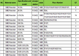
case001-1

Bom list

Detailed parameters and models of various electronic components and position numbers on PCB board are required

case00001

schematic diagram (SCH)

Customers who need secondary development and customers who need to improve or upgrade old products in the past need reverse schematic diagram

Why us?

Process for producing the finished product: fabrication of the PCB plates; production of the steel mesh; quotation for the purchase of components (provided during the 4-5 days spent fabricating the light board; concurrently, the customer may also supply raw materials); patching of the machine to produce the finished product; general cycle time: 10–12 days; if the customer is in a rush, please discuss with customer service to speed up the process.

  We are faster than our peers.

PCB board welding processing: Send us the printed circuit board files or physical photos of the board you wish to solder. Tell you how much you want to solder and ask for the front and back sides.

 Compared with peers, our charges are lower;

Circuit board copy board: You want to send us photos of the actual board; request the front and back; and specify the number of layers on the board and the number of required documents (general schematic SCH, circuit board diagram PCB, electronic bill of materials BOM).

 20 years of experience in PCB reverse engineering and engineer team;

Chip decryption: Send our customer service the chip model that needs to be unlocked directly.